一、 What is circuit board back drilling?
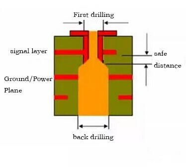
What is PCB circuit board back-drilling? In fact, back-drilling is a special type of deep-controlled drilling. In the production process of PCB multilayer boards, such as the production of 12-layer circuit boards, we need to connect the first layer to the ninth layer. , usually we drill through holes (one drill), and sink copper. In this way, the 1st floor is directly connected to the 12th floor. In fact, we only need to connect the 1st floor to the 9th floor. Since the 10th to the 12th floor are not connected by lines, they are like a pillar. This pillar affects the path of the signal, which can cause signal integrity problems in the communication signal. So drill out this extra pillar (called STUB in the industry) from the reverse side (secondary drilling). That’s why it’s called back-drilling, but generally it’s not so clean, because a little bit of copper will be electrolyzed in the subsequent process, and the drill tip itself is also sharp. Therefore, the circuit board manufacturer will leave a small point, and the length of the stub left is called the B value, which is generally in the range of 50-150UM.
What is circuit board back drilling
二、 What are the advantages of back drilling?
1. Reduce noise interference;
2. The local plate thickness becomes smaller;
3. Improve signal integrity;
4. Reduce the use of buried blind holes and reduce the difficulty of PCB circuit board manufacturing.
三、 What is the function of back drilling?
In fact, the function of back drilling is to drill out the PCB through-hole section that does not play any connection or transmission role, so as to avoid reflection, scattering, delay, etc. of high-speed signal transmission, and bring "distortion" to the signal. Research shows that it affects the signal integrity of the signal system In addition to factors such as design, PCB board material, transmission line, connector, chip packaging and other factors, via holes have a greater impact on signal integrity.
四、Working principle of back drilling production
Relying on the micro-current generated when the drill tip touches the copper foil on the substrate surface to sense the height of the board surface when the drill is drilled down, then drill according to the set drill-down depth, and stop when the drill-down depth is reached. As shown in Figure 2, the schematic diagram of the work
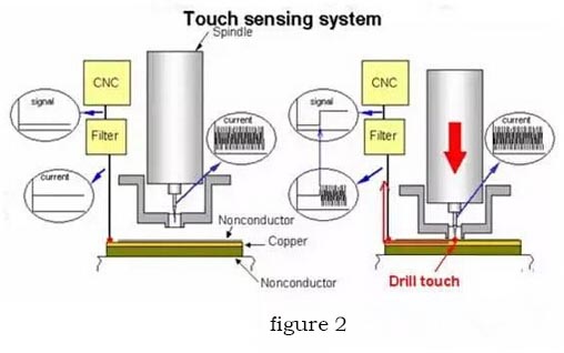
Working principle of back-drilling production
五, back-drilling production process?
1. First provide a circuit board with a positioning hole, and use the positioning hole to perform one-drill positioning and one-drilling of the PCB circuit board;
2. Electroplating the circuit board after a drill hole, and performing dry film sealing on the positioning hole before electroplating;
3. Make outer graphics on the electroplated circuit board;
4. Carry out pattern plating on the PCB circuit board after the outer pattern is formed, and perform dry film sealing on the positioning hole before pattern plating; The knife back-drills the plated holes that need to be back-drilled;
6. After back-drilling, wash the back-drilled hole with water to remove the remaining drill cuttings in the back-drilled hole.
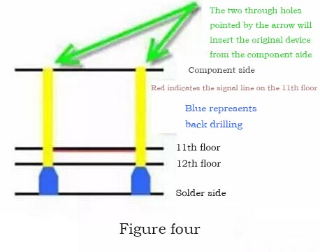
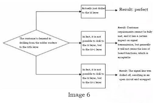
六. If there are holes in the circuit board and it is required to drill from the 14th layer to the 12th layer, how to solve it?
1. If the PCB board has signal lines on the 11th layer, there are through holes at both ends of the signal lines to connect to the component surface and the solder surface, and components will be inserted on the component surface, as shown in the figure below, that is to say , on this line, the transmission of the signal is from component A to component B through the signal line on the 11th layer.
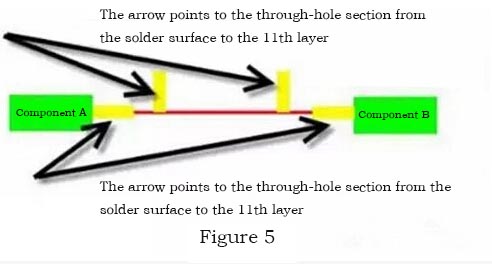
2. According to the signal transmission situation described in point 1, the function of the through hole in this transmission line is equivalent to that of the signal line. If we do not perform back drilling, the signal transmission route is shown in Figure 5.
Due to the certain tolerance control requirements of the drilling depth and the thickness tolerance of the plate, we cannot 100% meet the customer's absolute depth requirements, so is it better to control the depth of the back drilling? Deeper or shallower? Our view on the process It is better to be shallow than to be deep, Figure 6.
七、 What are the technical characteristics of the back drilling plate?
1. Most backplanes are rigid boards;
2. The thickness and diameter are relatively large;
3. The size of the PCB board is large;
4. Plate thickness: above 2.5mm;
5. Generally, the minimum hole diameter of the first drill is >=0.3mm;
6. Back drilling depth tolerance: +/-0.05MM;
7. The number of layers of PCB multilayer board - generally 8 to 50 layers;
8. The back drill hole is usually 0.2MM larger than the hole that needs to be drilled;
9. There are fewer outer layers, and most of them are designed as square arrays of crimping holes;
10. If the back-drilling requires drilling to the M layer, then the minimum thickness of the medium from the M layer to the M-1 (the next layer of the M layer) layer is 0.17MM
八、 What fields are back-drilled panels mainly used in?
Backplanes are mainly used in communication equipment, large servers, medical electronics, military, aerospace and other fields. Since military and aerospace are sensitive industries, domestic backplanes are usually provided by research institutes and R&D centers of military and aerospace systems or PCB manufacturers with strong military and aerospace backgrounds; in China, the demand for backplanes mainly comes from the communication industry, and now gradually Develop and expand the field of communication equipment manufacturing.
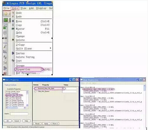
Realize back drilling file output in Allegro
1. First select the back drill Net and define the length. Click Edit-Properties in the menu bar to open the Editproperty dialog box, as shown below:
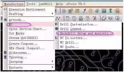
2. Click in the menu: Manufacturing→NC→BackdrillSetupandAnalysis, as shown below:
3. Back drilling can start from the top layer or from the bottom layer. The connection pins and VIA on the high-speed signal need to be back drilled. The settings are as follows:
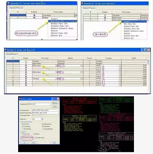
4. The drilling file is as follows:
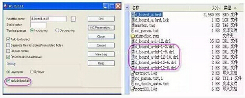
5. Package the back-drilling file and the back-drilling depth form to the PCB factory, and the back-drilling depth form needs to be filled in manually.
Some related properties
①.BACKDRILL_MAX PTH_STUB(net): In the constraintmanager, you need to assign the BACKDRILL_MAX_PTH_STUB attribute to the network of the back drill, and the software will only recognize it if the property is set.
Backdrilling needs to be considered for this network. In the constraintmanager→net-generalproperties→worksheet-backdil item, select the required item and click the right mouse button, select the change command in the pop-up shortcut menu, and enter the value of maximumstub. Stub calculation principle is that both top and bottom stubs will be included in the maximum stub length.
②.BACKDRILL_EXCLUDE attribute: After defining this attribute, the relevant target will not be back drilled. This attribute can be assigned to symbol, pin, via, and even attributes can be attached when building the database.
③.BACKDRILL_MIN_PIN_PTH attribute: Ensure the minimum depth of through-hole metallization
④.BACKDRILL_OVERRIDE property: user-defined range of backdrill, which is also a useful method, especially for designs with simple structure and consistent backdrill depth.
⑤.BACKDRILL_ PRESSFIT_CONNECTOR attribute: This is the setting attribute for the crimping parts. Generally, the back drill will identify the crimping device, and will not back drill from the device surface. If it is required to back drill on both sides.
If there is no problem in the analysis, then the settings of the back drill are all completed. You need to select include backdrill in the output stage of the post-processing light drawing, such as NC-Drillegend and NCDrill, and then execute to generate the back drill hole bitmap and drill file. .


